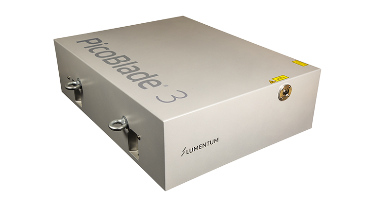
Lumentum high-power ultrashort-pulse lasers enable implementation of sustainable practices including manufacturing of solar cells. This market is a strongly growing market
with approximately 95% of commercial cells based on silicon wafer technology. Our micromachining lasers offer increased throughput and precision these manufacturing processes require.
Laser Contact Opening (LCO) for TOPCon
Gentle removal of dielectric layers with precise positioning at high speed
Laser contact opening for tunnel oxide passivated contact (TOPCon) solar cells requires reliable removal of the reflective dielectric coating on the cell’s rear side to establish good electrical contact without damaging the thin functional layers underneath. Nanosecond-pulse lasers – as typically used in standard PERC-production – are not suitable for TOPCon since they destroy the poly-silicon and tunnel-oxide layers. Ultrashort-pulse PicoBlade® lasers with green or ultraviolet emission on the other hand are ideal tools for this task: especially the UV wavelength as it limits the optical penetration-depth of the laser radiation to the dielectric layer only, while the short pulse-duration efficiently eliminates heat-induced damage to the underlying substrate. PicoBlade FlexBurst™ function, which enables flexible bursts with programmable amplitude of individual pulses, allows gentle ablation with maximum efficiency. Since the residual damage is extremely shallow, the thickness of the deposited amorphous silicon layer can be reduced which means a substantial cost-reduction. In addition, the laser’s AccuTrig™ function, operating up to 2 MHz pulse repetition rate, allows precise positioning of individual openings at scanning speeds of several ten meters per second.
Silver-Free Contacts
Reducing cost while improving performance
Screen-printed contacts based on silver-paste are costly and therefore reduce the margin on your product. Shallow laser-ablation of electrically insulating dielectric layers, whether on the front- or the rear side of the cell, enable economical nickel-copper (Ni-Cu) plated contacts to replace the silver. The high beam quality of PicoBlade ultrafast lasers facilitates small contact openings with <20 µm optical width, reducing the extend of the metal contact on the frontside and therefore maximizing the active area.
Hetero-Junction Technology (HJT)
Gentle laser contact opening for advanced HJT cell designs
Hetero-junction technology is the go-to technology for new entrants to the photovoltaics market as well as for established manufacturers to build out capacity. This is mainly due to HJT using a comparably simple and very energy-efficient manufacturing process. The cells offer high efficiency since they incorporate direct bandgap materials and exhibit a very low temperature coefficient. In addition, they are free of light induced degradation (LID) which promises improved efficiency over their lifetime.
While basic HJT architectures implement transparent conductive oxides (TCO) such as indium tin oxide (ITO) as capping layers on top of the functional amorphous silicon layers to establish electrical contact, more sophisticated designs add electrically insulating dielectric layers on top of the TCO to improve antireflective/reflective properties of the cell surfaces. To establish electrical contact, an LCO-process similar to the one used in TOPCon production is mandatory, not to destroy the nanometer-sized functional layers underneath. An additional laser-structured dielectric layer can also act as a mask to implement silver-free plated contacts.
Interdigitated Back Contact (IBC)
Precise positioning of laser contact openings with AccuTrig trigger functionality
IBC is a very rugged and mature cell architecture which offers very high efficiency. IBC cells can be easily identified by their undisturbed, metal contact-free front surface – shading losses are fully eliminated. All electrical contacts are located on the rear side of the cell. A pattern of p- and n-doped regions on the back side create the required p-n-junctions lateral to the cell’s surface rather than across the wafer. As with other high-efficiency cell architectures, IBC implements sophisticated, thin passivation layers and dielectric coatings which require gentle laser contact opening by an ultrashort pulsed laser. Due to the doping pattern, precise positioning of individual contact points is crucial. With the precision and accuracy that comes from Lumentum ultrashort pulsed lasers with patented AccuTrig technology, you can be sure to consistently receive the desired pattern with a position accuracy of 1 µm for scanning speeds of up to 40 m/s to perfectly align with the underlying structures.
